
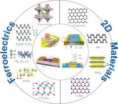
Discover how 2D ferroelectric in‑sensor computing devices like α‑In₂Se₃ and CIPS are reshaping sensor-memory-compute integration for ultra‑low power edge AI.
Have you ever wondered why your phone’s camera can process your face in real-time, or how future smart sensors might recognize traffic patterns instantly without a cloud connection? Enter 2D ferroelectric in‑sensor computing devices — emerging hardware that combines sensing, memory, and processing in a single slice of atomically thin material. By embedding computation right where data is captured, these devices have the potential to slash latency, power use, and hardware bulk.
With ever-growing demands from AI, IoT, self-driving cars, and neuromorphic systems, traditional architectures—separate sensing, storage, and computing—are starting to bottleneck. That’s where these 2D ferroelectric wonders step in: they sense light or voltage, store memory non‑volatily, and do basic “thinking” locally. It’s like giving sensors their own tiny brain.
What is ferroelectricity in two‑dimensional materials?
Broken symmetry and switchable dipoles
Ferroelectricity arises when crystal structures lack a center of symmetry, allowing the positive and negative charges to shift. In 2D materials, even just a single layer can hold a reversible electric polarization. Apply an electric field, and you switch that polarization—and it stays put until flipped again. That underpins non‑volatile memory. ScienceDirect+4RSC Publishing+4RSC Publishing+4MDPI
The unique advantage of 2D ferroelectrics? They maintain this switchable polarization at room temperature even at monolayer thickness, unlike most traditional bulk ferroelectric films. The layered van der Waals structure prevents surface defects and depolarization issues. MDPI+2RSC Publishing+2
Why 2D ferroelectrics make sense for in‑sensor computing
- Ultra-low power: switching dipoles at nanoscale consumes femto‑joules or less.
- Fast switching: polarization flips in nanoseconds.
- High retention & endurance: memory states last seconds to years, with cycle lifetimes reaching billions.
- Clean interfaces: 2D materials stack neatly without dangling bonds or lattice mismatches. RSC Publishing+1
Takeaway: 2D ferroelectric materials offer switchable, persistent memory and fast response in atomically thin form—perfect for embedded sensing and processing.
Types of 2D ferroelectric devices for in‑sensor computing
1. Intrinsic ferroelectric devices
Materials like α‑In₂Se₃, SnSe, SnS, and CuInP₂S₆ (CIPS) hold polarization within their crystal lattice—no stacking trick required. pubs.aip.org+7MDPI+7MDPI+7
- α‑In₂Se₃: each quintuple layer (Se–In–Se–In–Se) lacks symmetry, allowing both in‑plane and out‑of‑plane dipoles. The central Se atom “slides,” locking the dual directions. MDPI
- It can also sense visible light directly, thanks to its bandgap and internal polarization. One study even reports high photovoltaic currents under visible illumination—100× stronger than conventional ferroelectrics. RSC Publishing
- In synaptic memristor devices (α‑In₂Se₃ + SnSe), paired-pulse facilitation reached ~457%, enabling Pavlovian-style associative learning in hardware. RSC PublishingScienceDirect
- It can also sense visible light directly, thanks to its bandgap and internal polarization. One study even reports high photovoltaic currents under visible illumination—100× stronger than conventional ferroelectrics. RSC Publishing
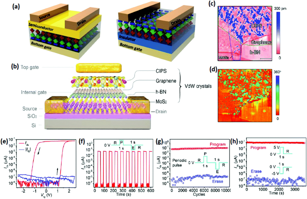
- CIPS (CuInP₂S₆): an insulating 2D ferroelectric with switchable out-of-plane polarization owing to Cu‑cation displacement. Its clean, dangling-bond‑free surface and high electroresistance make it ideal for memory and gate dielectric layers. RSC PublishingScienceDirect
- Used with a semiconductor like SnS₂ or graphene, it enables optoelectronic synaptic behavior and reservoir computing (RC) systems with MNIST recognition accuracies of ~93.6%. RSC Publishing
- Used with a semiconductor like SnS₂ or graphene, it enables optoelectronic synaptic behavior and reservoir computing (RC) systems with MNIST recognition accuracies of ~93.6%. RSC Publishing
Intrinsic 2D ferroelectrics combine sensing and memory in one material; α‑In₂Se₃ and CIPS have proven exceptionally effective in neuromorphic and edge sensing demos.
2. Interfacial ferroelectric devices
Here, a non-ferroelectric 2D channel (like MoS₂, WSe₂, MoTe₂, graphene) pairs with a traditional ferroelectric dielectric such as P(VDF‑TrFE), BaTiO₃, or HfO₂ / HfₓZr₁₋ₓO₂ (HZO). RSC Publishingoar.a-star.edu.sgMDPI
- Example: Graphene/MoTe₂ with a P(VDF‑TrFE) layer can be tuned between p–n and n–p homojunction states by flipping FE domains. This reverses photoresponse polarity and enables multi-level synaptic weights and reconfigurable convolutional kernels for edge detection. Arrays of these devices have shown pattern recognition and even robot control in real-time with ~10⁻¹³ J per operation. RSC PublishingRSC Publishing
- HZO‑based ferroelectric thin films: CMOS‑compatible and scalable below 10 nm thickness. When integrated with MoS₂/WSe₂, they deliver sub‑60 mV/dec subthreshold swings, sub‑picojoule per spike energy, nanosecond switching (~4.8 ns), retention over 10 years, and endurance over 10¹³ cycles. RSC Publishingoar.a-star.edu.sg
Interfacial FE devices harness the best of both worlds—sensitive 2D channels and scalable ferroelectric dielectrics—to create low‑power synaptic devices for neuromorphic, edge, and in‑sensor computing.
3. Interlayer ferroelectric devices (sliding or moiré‑induced)
Polarization can also emerge between stacked layers via asymmetry in twist or sliding alignment—creating interlayer-induced ferroelectricity. link.aps.orgScienceDirectRSC Publishing
- Sliding bilayer MoS₂: in the 3R stack, shear between layers displaces charge centers, flipping polarization. These FETs can operate at sub‑3 nm node scales. RSC PublishingScienceDirect
- Moiré trilayer graphene/h-BN structures: asymmetrically twisted moiré patterns give rise to excitonic or electronic ratchet states. These devices achieve conductance memory at ultra-low power (20 pW), fast switching, and neuromorphic-like adaptation. Photodetectors based on twisted double bilayer graphene achieve mid‑IR photovoltaic responsivity (3.7 V/W) at long wavelengths like 5 μm. RSC PublishingScienceDirect
H3 Takeaway: When you let layers slide or twist, weird but useful ferroelectric behavior emerges—building memory, sensing and computing in an emergent nano‑stack.
Capabilities in real‑world applications
⚡ Case study A: In‑sensor Pavlovian learning via α‑In₂Se₃/SnSe junctions
Imagine a sensor that learns like Pavlov’s dog—beginning with no response to a weak stimulus, but after paired light and electrical pulses it begins to respond to the light alone.
- This is exactly how a junction of α‑In₂Se₃ and SnSe behaves: starting with a sub-threshold electric pulse (conditioned stimulus), no response; after five pairings with optical pulses (unconditioned stimulus), the junction triggers suprathreshold current autonomously from electrical pulses alone.
- Paired-pulse facilitation peaked at ~457% and current increases remained for extended retention—mimicking synaptic learning in hardware. RSC PublishingScienceDirect
📸 Case study B: MoS₂/CIPS reservoir computing systems
Reservoir computing (RC) mimics part of the brain’s processing: inputs pass through a “reservoir” that transforms them non‑linearly, and outputs get classified after training.
- Fe‑FETs made by combining SnS₂ or MoS₂ with CIPS dielectric layers act as optoelectronic synapses: light induces short-term potentiation (STP) in currents, while electrical pulses give long-term potentiation (LTP) and depression.
- A fully 2D RC architecture achieved 93.62% accuracy on MNIST digit recognition—using significantly less energy and less area than conventional digital systems. RSC Publishing
🤖 Case study C: Edge detection with reconfigurable graphene/MoTe₂ homojunctions
- A gate-controlled P(VDF‑TrFE) ferroelectric layer under graphene/MoTe₂ allows dynamic switching of p–n vs. n–p regions—thus flipping photoresponse polarity.
- This enables a 3×3 cell array to behave like a programmable convolutional kernel—able to detect edges, perform pattern classification, and even direct a robotic dog in real-time—all with ~10⁻¹³ J per operation. RSC PublishingRSC Publishing
🧩 Case study D: HZO/MoS₂ steep‑slope Fe‑FETs
- With CMOS-compatible HfₓZr₁₋ₓO₂ dielectric layers and MoS₂, devices achieve sub-60 mV/dec switching, nanosecond write/erase times (~4.8 ns), retention >10 years, and endurance of over 10¹³ cycles.
- Such devices enable ultra‑low‑power spiking operations ideal for neuromorphic spikes and on-device memory. RSC Publishingoar.a-star.edu.sg
🛠 Key advantages, challenges, and tips for developers in India
Advantages
- Compact integration: sensing + memory + computing in inches of atomically thin stacks.
- Energy frugality: femto- to picojoule operations at sub-nanosecond speeds—ideal for battery-operated edge devices.
- Neuromorphic learning: built-in synaptic behavior like STP/LTP without external training hardware.
- Room-temperature stability: most devices operate robustly at 300 K or above.
- Fabrication scalability: emerging techniques enable wafer-scale growth of α‑In₂Se₃ and other 2D materials. polyu.edu.hk
Challenges
- Scalable synthesis: producing large-area, high-purity monolayers (e.g. α‑In₂Se₃) without defects remains painstaking. New TEM‑guided methods show promise. polyu.edu.hkScienceDirect
- Environmental stability: many 2D materials oxidize unless passivated or capped—necessitating clean-room fabrication and encapsulation.
- Device variability: subtle layer-to-layer misalignment or interface roughness may cause inconsistent polarization switching.
- Integration with silicon: blending 2D ferroelectric components with CMOS or conventional electronics demands careful alignment and thermal matching.
Tips for Indian researchers & startups
- Partner with institutions like IITs or IISc with 2D materials expertise and advanced TEM facilities—it accelerates material discovery and device testing.
- Start with simple Fe‑FET prototypes using α‑In₂Se₃ / MoS₂ or CIPS / MoS₂ stacking, focusing first on synaptic behavior metrics like PPF, STP/LTP balance.
- Consider collaborators skilled in optical characterization to benchmark photovoltaic responses (bulk PV, responsivity, retention).
- Look into hybrid platforms combining ferroelectric MoS₂ with HZO layers—bridging CMOS-integration with edge inference.
- Test devices in India’s environmental conditions (humidity, temperature), and explore local packaging or encapsulation solutions.
Summary & key takeaways
- Intrinsic ferroelectrics like α‑In₂Se₃ and CIPS can sense light and store memory in one material layer. Best for neuromorphic, associative learning and reservoir computing.
- Interfacial ferroelectrics use sensitive 2D channels and scalable thin-film dielectrics like P(VDF‑TrFE) or HZO, enabling edge detection, reconfigurable photoresponsivity, and deep-edge AI.
- Interlayer or sliding ferroelectrics deliver exotic, moiré‑driven memory/sensing behavior at ultra-low power—great for future quantum or compact neuromorphic hardware.
- Applications demonstrated include Pavlovian learning circuits, edge detection for robotics, digit recognition with RC, and steep‑slope Fe‑FETs suitable for AI‑edge accelerators.
- Key challenges lie in scalable 2D material synthesis, integration stability, and aging under real‑world conditions—areas where Indian labs can make major contributions.
✅ Call to Action
Have you worked on 2D materials or neuromorphic hardware? What’s your take on merging sensing, memory and compute in one slice of material? Share your thoughts or experience below—let’s spark a conversation on how 2D ferroelectric in‑sensor computing devices can transform AI and electronics right here in India 🇮🇳.
Leave a Reply